


Artículos SCI
2022
2022
Materiales Nanoestructurados y Microestructura
Ultrathin Plasma Polymer Passivation of Perovskite Solar Cells for Improved Stability and Reproducibility
Obrero-Perez, JM; Contreras-Bernal, L; Nuñez-Galvez, F; Castillo-Seoane, J; Valadez-Villalobos, K; Aparicio, FJ; Anta, JA; Borras, A; Sanchez-Valencia, JR; Barranco, AAdvanced Energy Materials, (2022) 2200812 DOI: 10.1002/aenm.202200812
Abstract
Despite the youthfulness of hybrid halide perovskite solar cells, their efficiencies are currently comparable to commercial silicon and have surpassed quantum-dots solar cells. Yet, the scalability of these devices is a challenge due to their low reproducibility and stability under environmental conditions. However, the techniques reported to date to tackle such issues recurrently involve the use of solvent methods that would further complicate their transfer to industry. Herein a reliable alternative relaying in the implementation of an ultrathin plasma polymer as a passivation interface between the electron transport layer and the hybrid perovskite layer is presented. Such a nanoengineered interface provides solar devices with increased long-term stability under ambient conditions. Thus, without involving any additional encapsulation step, the cells retain more than 80% of their efficiency after being exposed to the ambient atmosphere for more than 1000 h. Moreover, this plasma polymer passivation strategy significantly improves the coverage of the mesoporous scaffold by the perovskite layer, providing the solar cells with enhanced performance, with a champion efficiency of 19.2%, a remarkable value for Li-free standard mesoporous n-i-p architectures, as well as significantly improved reproducibility.
Julio, 2022 · DOI: 10.1002/aenm.202200812
Fotocatálisis Heterogénea: Aplicaciones
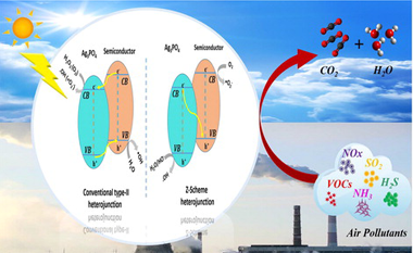
Photocatalytic oxidation of pollutants in gas-phase via Ag3PO4-based semiconductor photocatalysts: Recent progress, new trends, and future perspectives
Y. Naciri; A. Hsini; A. Bouziani; R. Djellabi; Z. Ajmal; M. Laabd; J.A. Navío; A. Mills; C.L. Bianchi; H.Li; B. Bakiz; A. AlbourineCritical Reviews in Environmental Science and Technology, 52 (2022) 2339-2382 DOI: 10.1080/10643389.2021.1877977
Abstract
Air pollution has become a significant challenge for both developing and developed nations. due to its close association with numerous fatal diseases such as cancer, respiratory, heart attack, and brain stroke. Over recent years, heterogeneous semiconductor photocatalysis has emerged as an effective approach to air remediation due to the ease of scale-up, ready application in the field, use of solar light and ready availability of a number of different effective photocatalysts. To date, most work in this area has been conducted using UV-absorbing photocatalysts, such as TiO2 and ZnO; However, recent studies have revealed Ag3PO4 as an attractive, visible-light-absorbing alternative, with a bandgap of 2.43 eV. In particular, this material has been shown to be an excellent photocatalyst for the removal of many types of pollutants in the gas phase. However, the widespread application of Ag3PO4 is restricted due to its tendency to undergo photoanodic corrosion and the poor reducing power of its photogenerated conductance band electrons, which are unable to reduce O2 to superoxide •O2 −. These limitations are critically evaluated in this review. In addition, recent studies on the modification of Ag3PO4 via combination with the conventional heterojunctions or Z-scheme junctions, as well as the photocatalytic mechanistic pathways for enhanced gas-pollutants removal, are summarized and discussed. Finally, an overview is given on the future developments that are required in order to overcome these challenges and so stimulate further research into this promising field.
Julio, 2022 · DOI: 10.1080/10643389.2021.1877977
Química de Superficies y Catálisis
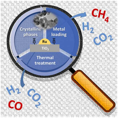
The effect of support surface hydroxyls on selective CO methanation with Ru based catalysts
Martínez, LMT; Muñoza, A; Pérez, A; Laguna, OH; Bobadilla, LF; Centeno, MA; Odriozola, JAApplied Catalysis A: General, 641 (2022) 118678 DOI: 10.1016/j.apcata.2022.118678
Abstract
The aim of this work was to clarify the effect of the support on CO selective methanation with Ru/TiO2 catalysts. TPR, XRD and TEM measurements confirmed that the changes in the activity and selectivity should be ascribed to anatase:rutile ratio, RuO2 +TiO2 solid solution formation, as well as the metal content and the thermal treatment used. All these characteristics result in active and selective catalysts in which the suppression of the reverse water gas shift reaction was observed. The catalytic performance must be explained by both the formation of more active Ru species as a result of support influence and the higher Ru dispersion. The study allows to conclude that for CO activation the role of support surface hydroxyls seems to be determinant for both the activity and selectivity of Ru/TiO2 catalysts.
Julio, 2022 · DOI: 10.1016/j.apcata.2022.118678
Materiales de Diseño para la Energía y Medioambiente
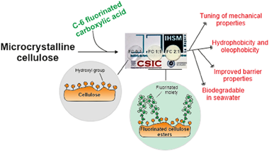
Greaseproof, hydrophobic, and biodegradable food packaging bioplastics from C6-fluorinated cellulose esters
Guzman-Puyol, S; Tedeschi, G; Goldoni, L; Benitez, JJ; Ceseracciu, L; Koschella, A; Heinze, T; Athanassiou, A; Heredia-Guerrera, JAFood Hydrocolloids, 128 (2022) 107562 DOI: 10.1016/j.foodhyd.2022.107562
Abstract
Tridecafluorononanoic acid (TFNA), a C6-fluorinated carboxylic acid, was esterified with cellulose at different molar ratios (0:1, 1:1, 2:1, and 3:1) in a trifluoroacetic acid (TFA):trifluoroacetic anhydride (TFAA):CHCl3 (2:1:1, v:v:v) solvent mixture. Free-standing films were obtained for all formulations and are presented as alternatives to composites and blends of paper with fluorinated molecules. Mechanical properties were investigated by tensile tests, and a plasticizer effect of fluorinated chains was observed. Interestingly, the wettability of these new cellulose derivatives was similar or even better than other common cellulose derivatives and fluorinated poly-mers employed in food packaging. Hydrodynamic properties were also improved by addition of TFNA, resulting in materials with water vapor permeability values comparable to other cellulose-based food packaging materials. In addition, films with the higher amounts of TFNA showed the required oil resistance for papers used in food packaging applications, as determined by the Kit Test. Finally, the biodegradation of these C6-fluorinated cel-lulose esters, assessed by biological oxygen demand (BOD) in seawater, was higher than typical bio-based polymers used in food packaging. The bioplastic synthesized at a molar ratio 1:1 (TFNA:cellulose) showed excellent performances in terms of greaseproof, hydrophobicity, ductility, and biodegradability, representing a sustainable alternative to typical plastics used in food packaging.
Julio, 2022 · DOI: 10.1016/j.foodhyd.2022.107562
Química de Superficies y Catálisis
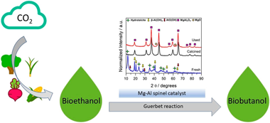
Insights on Guerbet Reaction: Production of Biobutanol From Bioethanol Over a Mg-Al Spinel Catalyst
Crespo, MAP; Vidal-Barrero, F; Azancot, L; Reina, TR; Campoy, MFrontiers in Chemistry, 10 (2022) 945596 DOI: 10.3389/fchem.2022.945596
Abstract
The production of biobutanol from bioethanol by the Guerbet reaction is an alternative pathway to renewable sources. The commercial viability of this green route requires improvements in the process development. This study experimentally examines the influence of operating conditions on the performance of a Mg-Al spinel catalyst prepared from hydrotalcite precursors. This catalyst demonstrates an exceptional performance in the Guerbet reaction with a promising activity/butanol selectivity balance, excellent long-term stability, and very-low-carbon footprint (CO2 generation as by-products is minimal). This study showcases a systematic strategy to optimize the reaction parameters in the Guerbet reaction for biobutanol production using an advanced spinel catalyst. Upon carefully adjusting temperature, pressure, space velocity, and reactants co-feeding, very promising conversion (35%) and butanol selectivity values (48%) were obtained.
Julio, 2022 · DOI: 10.3389/fchem.2022.945596
Reactividad de Sólidos
Steam-enhanced calcium-looping performance of limestone for thermochemical energy storage: The role of particle size
Arcenegui-Troya, J.; Sánchez-Jiménez, PE; Perejon, A; Valverde, JM; Pérez-Maqueda, LAJournal of Energy Storage, 51 (2022) 104305 DOI: 10.1016/j.est.2022.104305
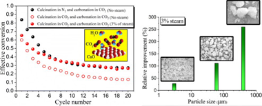
Abstract
Steam injection has been proposed to attenuate the decay of CaO reactivity during calcium looping (CaL) under operating conditions compatible with carbon capture and storage. However, it is yet unknown whether the perceived advantages granted by steam hold under the distinct operating conditions required for the integration of the CaL process as a thermochemical energy storage system in Concentrating Solar Power Plants (CaL-CSP). Here, we study the influence of steam in conditions compatible with a CaL-CSP scheme and assess its impact when injected only during one stage; either calcination or carbonation, and also when it is present throughout the entire loop. The results presented here demonstrate that steam boosts the CaO multicycle performance in a CO2 closed loop to attain residual conversion values similar to those achieved at moderate temperatures under inert gas. Moreover, it is found that the enhancement in multicycle activity is more pronounced for larger particles.
Julio, 2022 · DOI: 10.1016/j.est.2022.104305
Química de Superficies y Catálisis
Catalytic reforming of model biomass-derived producer gas
Azancot, L; Bobadilla, LF; Centeno, MA; Odriozola, JAFuel, 320 (2022) 123843 DOI: 10.1016/j.fuel.2022.123843
Abstract
This work includes a complete study of the reaction of reforming a simulated producer gas stream comparing a Ni-based catalyst with another one promoted with potassium to enhance the resistance to coke formation. Although coke deposition is unavoidable in the presence of tars in the stream, the analysis of different reaction parameters revealed that operating at 750 degrees C, weight hourly space velocity (WHSV) of 60 L-1 g(-1) h(-1) and 10-20 vol% of steam is possible to minimize the accumulation of carbon deposits. Moreover, it was demonstrated that the addition of potassium helps to mitigate carbon formation, but a high concentration of steam leads to nickel sintering and/or partial oxidation of metallic nickel. On this basis, it was successfully evidenced that the Ni-K catalyst is an excellent candidate for obtaining clean syngas from producer gas reforming.
Julio, 2022 · DOI: 10.1016/j.fuel.2022.123843
Materiales Ópticos Multifuncionales
Effect of Spatial Inhomogeneity on Quantum Trapping
Esteso, V; Carretero-Palacios, S; Miguez, HJournal of Physical Chemistry Letters, 13 (2022) 4513-4519 DOI: 10.1021/acs.jpclett.2c00807
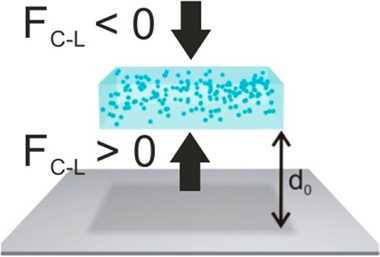
Abstract
An object that is immersed in afluid and approaching a substrate mayfind apotential energy minimum at a certain distance due to the balance between attractive and repulsiveCasimir-Lifshitz forces, a phenomenon referred to as quantum trapping. This equilibriumdepends on the relative values of the dielectric functions of the materials involved. Herein, westudy quantum trapping effects in planar nanocomposite materials and demonstrate that they arestrongly dependent on the characteristics of the spatial inhomogeneity. As a model case, weconsider spherical particles embedded in an otherwise homogeneous material. We propose aneffective medium approximation that accounts for the effect of inclusions andfind that anunprecedented and counterintuitive intense repulsive Casimir-Lifshitz force arises as a result ofthe strong optical scattering and absorption size-dependent resonances caused by their presence. Our results imply that the properanalysis of quantum trapping effects requires comprehensive knowledge and a detailed description of the potential inhomogeneity(caused by imperfections, pores, inclusions, and density variations) present in the materials involved
Junio, 2022 · DOI: 10.1021/acs.jpclett.2c00807
Nanotecnología en Superficies y Plasma
Titania Enhanced Photocatalysis and Dye Giant Absorption in Nanoporous 1D Bragg Microcavities
Rico, VJ; Turk, H; Yubero, F; González-Elipe, ARACS Applied Nano Materials, 5 (2022) 5487-5497 DOI: 10.1021/acsanm.2c00477
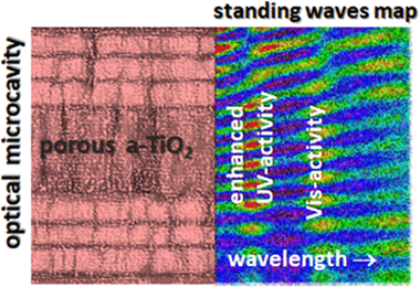
Abstract
Light trapping effects are known to boost the photocatalytic degradation of organic molecules in 3D photonic structures of anatase titania (a-TiO2) with an inverse opal configuration. In the present work, we show that photocatalytic activity can also be enhanced in a-TiO2 thin films if they are incorporated within a nanoporous 1D optical resonant microcavity. We have designed and manufactured multilayer systems that, presenting a high open porosity to enable a straightforward diffusion of photodegradable molecules, provide light confinement effects at wavelengths around the absorption edge of photoactive a-TiO2. In brief, we have observed that a nanoporous 1D Bragg microcavity prepared by electron beam evaporation at oblique angles comprising a central defect layer of nanoporous a-TiO2 boosts the photocatalytic degradation of nitrobenzene and methyl orange dye solutions. The multilayer structure of the microcavity was designed to ensure the appearance of optical resonances at the a-TiO2 layer location and wavelengths around the absorption onset of this semiconductor. In this porous 1D Bragg microcavity, the diffusion constraints of molecules through the capping layers covering the a-TiO2 are effectively compensated by an increase in the photocatalytic activity due to the light confinement phenomena. We also report that the absorption coefficient of methyl orange dye solution infiltrated within the pore structure of the microcavity is exalted at the wavelengths of the corresponding optical resonances. This effect gives rise to a small but non-negligible visible light photodegradation of dye molecules. The possibilities of tailoring the design of 1D photonic systems to boost the photocatalytic activity of a-TiO2 are discussed.
Junio, 2022 · DOI: 10.1021/acsanm.2c00477
Reactividad de Sólidos
Thermal behavior of ammonium fluorosilicates complexes: Obtaining and kinetic analysis
Resentera, AC; Perejon, A; Esquivel, MR; Perez-Maqueda, LA; Rodriguez, MHChemical Engineering Research amd Design, 182 (2022) 490-501 DOI: 10.1016/j.cherd.2022.04.021
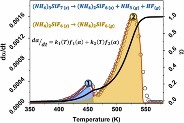
Abstract
In this work, a mixture of (NH4)3SiF7/(NH4)2SiF6 powders was obtained as a by-product of the Li extraction process from alpha-spodumene aluminosilicate with NH4HF2. The thermal behavior of the powders was analyzed by non-isothermal thermogravimetric experiments. The kinetic parameters that describe the processes involved were obtained using mathematical deconvolution, Friedman's method, combined kinetic analysis, and nonlinear regression optimization. The results show that the process occurs in two partially overlapping steps, the thermal decomposition of (NH4)3SiF7 into (NH4)2SiF6 and the subsequent sublimation of (NH4)2SiF6. The apparent activation energies were 72.6 and 79.8 kJ/ mol for steps 1 and 2, respectively. The apparent pre-exponential factors were 1.19 x 10⁶ and 2.50 x 10⁵ s-1, respectively. The kinetic models indicated that Step 1 follows an A2 model, while Step 2 follows an F0 model. Finally, the resulting kinetic parameters allowed the reconstruction of the original experimental curves and obtaining predictions of curves recorded under other heating programs.
Junio, 2022 · DOI: 10.1016/j.cherd.2022.04.021
Materiales Avanzados
Thermal behaviour of the different parts of almond shells as waste biomass
Garzon, E; Arce, C; Callejon-Ferre, AJ; Perez-Falcon, JM; Sanchez-Soto, PJJournal of Thermal Analysis and Calorimetry, 147 (2022) 5023-5035 DOI: 10.1007/s10973-021-10940-x
Abstract
The main aim of this study is to investigate the thermal behaviour of the different parts of almond shells produced in an almond industry as a waste biomass. For this purpose, several experiments have been conducted under laboratory conditions. After removing the mature almonds, the waste raw materials subject of this study were treated with distilled water (10 min) and separated in several parts. Taking into account their physical characteristics, they were: (a) complete shells: exocarp, mesocarp and endocarp without grinding (Sample C); (b) ground samples of complete shells, sieved under 0.2 mm (Sample M); (c) hard layers of the endocarp (Sample E); (d) internal layers of the endocarp (Sample I); and (e) mature drupes (Sample P) or skin, being constituted by the flexible part of green colour (fresh form) or yellow (after drying). The thermal behaviour of all these sample materials has been investigated using a laboratory furnace, with determination of ash contents and mass loss by progressive heating (120 min of holding time). Elemental and DTA-TG/DTG analyses of selected sample materials have been carried out. Although a complete study can be very complex, a first approach has been performed in this investigation. Results on thermal decomposition of this biomass waste have been presented to emphasize the main differences between sample materials of almond shells. These results have demonstrated the influence of several parameters, such as the particle size, and previous treatments in the thermal behaviour of the different parts of the almond shells, as showed in this investigation. Structural analysis of almond shells allowed to determine lignin, cellulose and hemicellulose. From the lignin content, it has been predicted the higher heating value (18.24 MJkg(-1)) of this waste as by-product of industrial interest. Other linear correlations to calculate this parameter have been applied with similar results in all these samples.
Junio, 2022 · DOI: 10.1007/s10973-021-10940-x
Nanotecnología en Superficies y Plasma
Electron beam evaporated vs. magnetron sputtered nanocolumnar porous stainless steel: Corrosion resistance, wetting behavior and anti-bacterial activity
Bobaru, S; Rico-Gavira, V; Garcia-Valenzuela, A; Lopez-Santos, C; Gonzalez-Elipe, ARMaterials Today Communications, 31 (2022) 103266 DOI: 10.1016/j.mtcomm.2022.103266
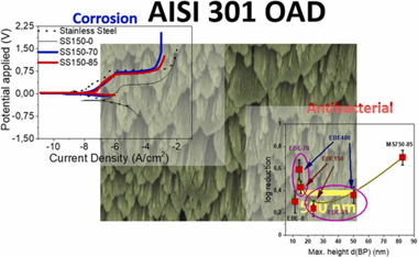
Abstract
Stainless steel (SS), widely used because of its outstanding corrosion protection properties, does not possess any particular anti-stain or anti-bacterial activity as required for household and sanitary applications. This work reports the fabrication of SS thin films that, keeping a similar corrosion resistance than the bulk material, presents hydrophobicity and anti-bacterial activity. These thin films are prepared at ambient temperature by physical vapor deposition (PVD), either electron beam evaporation (EBE) or magnetron sputtering (MS), at oblique angles (OAD). According to their scanning electron microcopy and atomic force microscopy analysis, the microstructure of the OAD-SS thin films consisted of tilted and separated nanocolumns defining a surface topology that, characterized by a high percentage of void space, varied with the deposition conditions and procedure, either EBE or MS. It has been shown that particularly the nanocolumnar MS-OAD thin films preserved and even improved the high corrosion resistance of compact SS, as determined by electrochemical analysis. Besides, all OAD-SS thin films depict hydrophobicity and a high antibacterial activity. These features, particularly remarkable for the MS-OAD thin films, have been related with their tip-like termination at the surface and the existence of large void spaces separating the nanocolumns. This topology appears to affect negatively the bacteria's deployment onto the surface and therefore the survival rate. Differences in the corrosion and antibacterial performance between EBE and MS-OAD thin films have been related with the specificities of these two PVD methods of thin film preparation. A relatively high abrasion resistance, as determined by abrasion tests, supports the use of MS-OAD thin films for the protection of commodity materials.
Junio, 2022 · DOI: 10.1016/j.mtcomm.2022.103266
Nanotecnología en Superficies y Plasma
Comparative analysis of the germination of barley seeds subjected to drying, hydrogen peroxide, or oxidative air plasma treatments
Perea-Brenes, A; Gomez-Ramirez, A; Lopez-Santos, C; Oliva-Ramirez, M; Molina, R; Cotrino, J; García, JL; Cantos, M; González-Elipe, ARAPlasma Processes and Polymers 19 (2022) e2200035 DOI: 10.1002/ppap.202200035
Abstract
Acceleration in germination time by 12-24 h for barley seeds treated with atmospheric air plasmas may have a significant economic impact on malting processes. In this study, the increase in germination rate and decrease in contamination level upon plasma treatment could not be directly correlated with any significant increase in the water uptake capacity, except for seeds exposed to mild drying treatment. A variety of germination essays have been carried out with seeds impregnated with an abscisic acid solution, a retarding factor of germination, treated with a peroxide solution, and/or subjected to the plasma and drying treatments. Results suggest that plasma and hydrogen peroxide treatments induce the formation of reactive oxygen and nitrogen species that affects the abscisic acid factor and accelerate the germination rate.
Junio, 2022 · DOI: 10.1002/ppap.202200035
Nanotecnología en Superficies y Plasma
Nanostructured nickel based electrocatalysts for hybrid ethanol-water anion exchange membrane electrolysis
Lopez-Fernandez, E; Gomez-Sacedon, C; Gil-Rostra, J; Espinos, JP; Gonzalez-Elipe, AR; Yubero, FJournal of Environmental Chemical Engineering, 10 (2022) 107994 DOI: 10.1016/j.jece.2022.107994
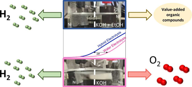
Abstract
Ni and Ni-Fe nanostructured layers prepared by magnetron sputtering in an oblique angle deposition configuration (MS-OAD) have been used as anode and cathode catalysts for hybrid ethanol-water electrolysis in an anion exchange membrane (AEM) electrolyser. Physico-chemical and electrochemical characterization in a threeelectrode cell has been carried out to determine the optimal characteristics of the anodic films. Current densities up to 434 mA cm-2 at 2.0 V in a 1.5 M EtOH and 2.0 M KOH fuel solution were achieved with excellent operational stability for 3 days. These experiments show that the oxygen evolution reaction taking place at the anode is completely replaced by the ethanol oxidation reaction under our explored reaction conditions. The obtained results evidence the interest of this kind of organic vs. pure water electrolysis to decrease the overall electrical energy consumption for the production of hydrogen.
Junio, 2022 · DOI: 10.1016/j.jece.2022.107994
Fotocatálisis Heterogénea: Aplicaciones
Pursuing efficient systems for glucose transformation to levulinic acid: Homogeneous vs. heterogeneous catalysts and the effect of their co-action
Bounoukta, CE; Megias-Sayago, C; Ivanova, S; Ammari, F; Centeno, MA; Odriozola, JAFUEL, 318 (2022) 123712 DOI: 10.1016/j.fuel.2022.123712
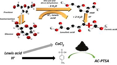
Abstract
Exploring available catalytic systems to understand their behavior is a must to properly design efficient catalysts aiming to definitively drive biomass from laboratory to industrial scale. Glucose transformation to levulinic acid involves cascade reactions with specific requirements, different active sites in each case and secondary reactions hard to avoid which are intrinsically linked to the catalyst's nature and reaction conditions. In the present work, homogeneous, heterogeneous and heterogeneous/homogeneous catalysts are considered with the unique goal of improving levulinic acid yield while understanding the catalytic behaviour of cost-effective catalysts. The choice of the catalytic systems and the effect of the main reaction parameters on activity and selectivity is studied and discussed.
Junio, 2022 · DOI: 10.1016/j.fuel.2022.123712
Materiales Avanzados
Vitrification rate and estimation of the optimum firing conditions of ceramic materials from raw clays: A review
Garzon, E; Perez-Villarejo, L; Eliche-Quesada, D; Martinez-Martinez, S; Sanchez-Soto, PJCeramics International, 48 (2022) 15889-15898 DOI: 10.1016/j.ceramint.2022.02.129
Abstract
The present work is a review concerning the previous investigations on the vitrification behaviour of clays containing kaolinite, feldspars, muscovite (illite/sericite) and pyrophyllite. These clays are silico-aluminous and have interesting properties as raw materials for structural ceramics. The mineralogical and chemical composition were determined. Then, the vitrification in these clay samples using pressed bodies was investigated by few researchers in the temperature range 800-1350 degrees C with 0.5-5.5 h of soaking times. The effect of heat treatments on the degree of vitrification in these clays was characterized by bulk densities of the ceramic bodies at the fired stage. It was found some variations of bulk density values for all these clays fired in the range 1000-1150 degrees C, with marked decreases of the values obtained at 1200 degrees C and 1300 degrees C. A first order reaction kinetics was applied to the analysis of vitrification of the ceramic bodies under isothermal heating. The method is based on experi-mental data of bulk densities, being proposed for the estimation of the relative degree of vitrification resulting from different firing schedules. The analysis considered the temperature dependence of the rate of vitrification following Arrhenius behaviour. Thus, the vitrification activation energy can be obtained. The activation energies for the physical process of vitrification in these clays ranged from 45 to 151 kJ/mol. The relative rates of vitrification or degree of vitrification attained during heating and soaking were calculated. The results suggested that the contribution of vitrification due to heating in all these clays was relatively small compared to the vitrification during soaking. However, it was evidenced that the influence of the particle sizes in the thermal behaviour of these clays cannot be neglected. The vitrification rate equations, as deduced in these previous studies, can be useful tools to estimate the optimum firing conditions of these clays, allowing the extension of this method to other clay types.
Junio, 2022 · DOI: 10.1016/j.ceramint.2022.02.129
Química de Superficies y Catálisis
Design of Full-Temperature-Range RWGS Catalysts: Impact of Alkali Promoters on Ni/CeO2
Gandara-Loe, J; Zhang, Q; Villora-Pico, JJ; Sepulveda-Escribano, A; Pastor-Perez, L; Reina, TREnergy & Fuels, 36 (2022) 6362-6373 DOI: 10.1021/acs.energyfuels.2c00784
Abstract
Reverse water gas shift (RWGS) competes with methanation as a direct pathway in the CO2 recycling route, with methanation being a dominant process in the low-temperature window and RWGS at higher temperatures. This work showcases the design of multi-component catalysts for a full-temperature-range RWGS behavior by suppressing the methanation reaction at low temperatures. The addition of alkali promoters (Na, K, and Cs) to the reference Ni/CeO2 catalyst allows identifying a clear trend in RWGS activation promotion in both low- and high-temperature ranges. Our characterization data evidence changes in the electronic, structural, and textural properties of the reference catalyst when promoted with selected dopants. Such modifications are crucial to displaying an advanced RWGS performance. Among the studied promoters, Cs leads to a more substantial impact on the catalytic activity. Beyond the improved CO selectivity, our best performing catalyst maintains high conversion levels for long-term runs in cyclable temperature ranges, showcasing the versatility of this catalyst for different operating conditions. All in all, this work provides an illustrative example of the impact of promoters on fine-tuning the selectivity of a CO2 conversion process, opening new opportunities for CO2 utilization strategies enabled by multi-component catalysts.
Junio, 2022 · DOI: 10.1021/acs.energyfuels.2c00784
Química de Superficies y Catálisis
Electrocatalytic CO2 conversion to C-2 products: Catalysts design, market perspectives and techno-economic aspects
Ruiz-López, E; Gandara-Loe, J; Baena-Moreno, F; Reina, TR; Odriozola, JARenewable & Sustainable Energy Reviews, 161 (2022) 112329 DOI: 10.1016/j.rser.2022.112329
Abstract
The energy crisis caused by the incessant growth in global energy demand joint to its associated greenhouse emissions motivates the urgent need to control and mitigate atmospheric CO2 levels. Leveraging CO2 as carbon pool to produce value-added products represents a cornerstone of the circular economy. Among the CO2 utilization strategies, electrochemical reduction of CO2 conversion to produce fuels and chemicals is booming due to its versatility and end-product flexibility. Herein most of the studies focused on C-1 products although C-2 and C2+ compounds are chemically and economically more appealing targets requiring advanced catalytic materials. Still, despite the complex pathways for C2+ products formation, their multiple and assorted applications have motivated the search of suitable electrocatalysts. In this review, we gather and analyse in a comprehensive manner the progress made regarding C2+ products considering not only the catalyst design and the electrochemistry features but also techno-economic aspects in order to envisage the most profitable scenarios. This state-of-the-art analysis showcases that electrochemical reduction of CO2 to C-2 products will play a key role in the decarbonisation of the chemical industry paving the way towards a low-carbon future.
Junio, 2022 · DOI: 10.1016/j.rser.2022.112329
Materiales y Procesos Catalíticos de Interés Ambiental y Energético
Enhanced photocatalytic activity of TiO2/WO3 nanocomposite from sonochemical-microwave assisted synthesis for the photodegradation of ciprofloxacin and oxytetracycline antibiotics under UV and sunlight
Moghni, N; Boutoumi, H; Khalaf, H; Makaoui, N; Colon, GJournal of Photochemistry and Photobiology A-Chemistry, 428 (2022) 113848 DOI: 10.1016/j.jphotochem.2022.113848
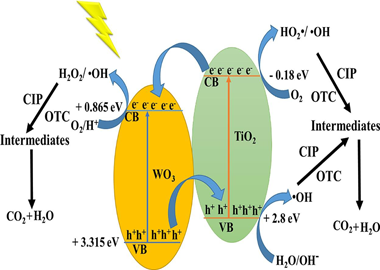
Abstract
The TiO2/WO3 photocatalysts were prepared by a simple assisted sonochemical -microwave combination. The wide surface and structural characterization of synthesized material confirmed that the adopted preparation method resulted in nanoparticulated crystallite anatase phase of TiO2 with a large surface area (> 200 m(2)/g), and the dispersion of WO3 on the surface of TiO2. The photoactivity was assessed for the photodegradation of ciprofloxacin (CIP) and oxytetracycline (OTC) antibiotics under UV and sunlight irradiation. The mineralization rate, toxicity assessment, pollutant concentration effect on photodegradation efficiency, and reusability potential under sunlight were all investigated. Results showed that TiO2 doped with 5 wt% of WO3 exhibited the best photocatalytic activity under UV (100% degradation) and solar light. Rate constants for CIP and OTC degradation showed that TiO2/WO3 significantly improved with respect to bare TiO2. The antibacterial study revealed that the photodegraded solutions became less toxic than the initial CIP and OTC solutions showing a significant decrease in the inhibition zone diameter and mineralization rates. The prepared TiO2/WO3 maintained high performances in the presence of high concentrations of pollutants as well as good stability after four consecutive uses. The increased photocatalytic activity is attributed to the incorporation of WO3, which extends the light absorption range and decreases the rate of electron -hole recombination.
Junio, 2022 · DOI: 10.1016/j.jphotochem.2022.113848
Química de Superficies y Catálisis
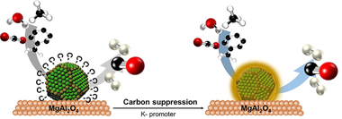
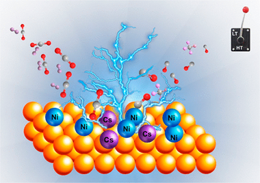
Evidence of new Ni-O-K catalytic sites with superior stability for methane dry reforming
Azancot, L; Blay, V; Blay-Roger, R; Bobadilla, LF; Penkova, A; Centeno, MA; Odriozola, JAApplied Catalysis B-Environmental, 307 (2022) 121148 DOI: 10.1016/j.apcatb.2022.121148
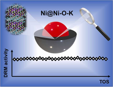
Abstract
Liquid fuels produced via Fischer-Tropsch synthesis from biomass-derived syngas constitute an attractive and sustainable energy vector for the transportation sector. This study focuses on the role of potassium as a promoter in Ni-based catalysts for reducing coke deposition during catalytic dry reforming. The study provides a new structural link between catalytic performance and physicochemical properties. We identify new Ni-O-K chemical states associated with high stability in the reforming process, evidenced by different characterization techniques. The nickel particles form a core surrounded by a Ni-O-K phase layer (Ni@Ni-O-K) during the reduction of the catalyst. This phase likely presents an alkali-nickelate-type structure, in which nickel is stabilized in oxidation state + 3. The Ni-O-K formation induces essential changes in the electronic, physical, structural, and morphological properties of the catalysts, notably enhancing their long-term stability in dry reforming. This work thus provides new directions for designing more efficient catalysts for sustainable gas-to-liquids processes.
Junio, 2022 · DOI: 10.1016/j.apcatb.2022.121148
Reduction of N2O with hydrosilanes catalysed by RuSNS nanoparticles
Molinillo, P; Lacroix, B; Vattier, F; Rendon, N; Suarez, A; Lara, PChemical Communications DOI: 10.1039/d2cc01470j
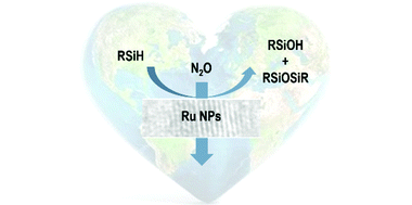
Abstract
A series of RuSNS nanoparticles, prepared by decomposition of Ru(COD)(COT) with H-2 in the presence of an SNS ligand, have been found to catalyse the reduction of the greenhouse gas N2O to N-2 employing different hydrosilanes.
Junio, 2022 · DOI: 10.1039/d2cc01470j
Materiales Avanzados
Synthesis and characterization of alkali-activated materials containing biomass fly ash and metakaolin: effect of the soluble salt content of the residue
Jurado-Contreras, S; Bonet-Martínez, E; Sánchez-Soto, PJ; Gencel, O; Eliche-Quesada, DArchives of Civil and Mechanical Engineering, 22 (2022) 121 DOI: 10.1007/s43452-022-00444-2
Abstract
The present study investigates the production and characterization of alkali-activated bricks prepared with mixing metakaolin (MK) and biomass fly ash from the combustion of a mix of pine pruning, forest residues and energy crops (BFA). To use this low cost and high availability waste, different specimens were prepared by mixing MK with different proportions of BFA (25, 50 and 75 wt%). Specimens containing only metakaolin and biomass fly ash were produced for the purpose of comparison. Effects of the alkali content of biomass fly ash, after a washing pretreatment (WBFA), as well as the concentration of NaOH solution on the physical, mechanical and microstructural properties of the alkali-activated bricks were studied. It was observed that up to 50 wt% addition of the residue increases compressive strength of alkali-activated bricks. Alkalinity and soluble salts in fly ash have a positive effect, leading materials with the improved mechanical properties. Concentration of NaOH 8 M or higher is required to obtain optimum mechanical properties. The compressive strength increases from 23.0 MPa for the control bricks to 44.0 and 37.2 MPa with the addition of 50 wt% BFA and WBFA, respectively, indicating an increase of more than 60%. Therefore, the use of biomass fly ash provides additional alkali (K) sources that could improve the dissolution of MK resulting in high polycondensation. However, to obtain optimum mechanical properties, the amount of BFA cannot be above 50 wt%.
Mayo, 2022 · DOI: 10.1007/s43452-022-00444-2
Materiales Coloidales
Neodymium doped lanthanide fluoride nanoparticles as contrast agents for luminescent bioimaging and X-ray computed tomography
Gonzalez-Mancebo, D; Becerro, AI; Calderon-Olvera, RM; Cantelar, E; Corral, A; Balcerzyk, M; De la Fuente, JM; Ocaña, MBoletin de la Sociedad Española de Ceramica y Vidrio, 61 (2022) 540-549 DOI: 10.1016/j.bsecv.2021.07.004
Abstract
The synthesis of uniform neodymium-doped lanthanum trifluoride nanoparticles with lenticular shape and a mean diameter around 45 nm by using a homogeneous precipitation method is reported. The luminescent properties of the synthesized samples in terms of their emission spectra and emission lifetime are analyzed as a function of the Nd content to find the optimum phosphor and its suitability for luminescent imaging in the second biological window. The X-ray attenuation properties of the optimum phosphor are evaluated to investigate their additional ability as contrast agent for X-ray computed tomography. Finally, the colloidal stability of the obtained nanoparticles in physiological medium and their cytotoxicity are also analyzed to assess their aptness for in vivo bioimaging applications.
Mayo, 2022 · DOI: 10.1016/j.bsecv.2021.07.004
Química de Superficies y Catálisis
Versatile Ni-Ru catalysts for gas phase CO2 conversion: Bringing closer dry reforming, reverse water gas shift and methanation to enable end-products flexibility
Merkouri, LP; le Sache, E; Pastor-Perez, L; Duyar, MS; Reina, TRFuel, 315 (2022) 123097 DOI: 10.1016/j.fuel.2021.123097
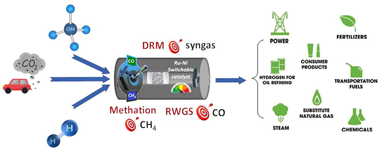
Abstract
Advanced catalytic materials able to catalyse more than one reaction efficiently are needed within the CO2 utilisation schemes to benefit from end-products flexibility. In this study, the combination of Ni and Ru (15 and 1 wt%, respectively) was tested in three reactions, i.e. dry reforming of methane (DRM), reverse water-gas shift (RWGS) and CO2 methanation. A stability experiment with one cycle of CO2 methanation-RWGS-DRM was carried out. Outstanding stability was revealed for the CO2 hydrogenation reactions and as regards the DRM, coke formation started after 10 h on stream. Overall, this research showcases that a multicomponent Ni-Ru/CeO2 -Al2O3 catalyst is an unprecedent versatile system for gas phase CO2 recycling. Beyond its excellent performance, our switchable catalyst allows a fine control of end-products selectivity.
Mayo, 2022 · DOI: 10.1016/j.fuel.2021.123097
Effect of sintering under CO+N-2/H-2 and CO2+air atmospheres on the physicochemical features of a commercial nano-YSZ
Colomer, M.T.; Simenas, M.; Banys, J.; Vattier, F.; Gagor, A.; Maczka, M.Journal of Alloys and Compounds, 904 (2022) 163976 DOI: 10.1016/j.jallcom.2022.163976
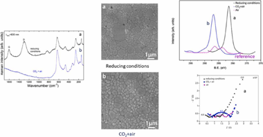
Abstract
Given the need to process anodes and composites based on nano-YSZ in reducing or in air containing additional CO2 atmospheres for the fabrication of solid oxide fuel cells (SOFCs), and solid oxide electrolysis cells (SOECs), we have studied the effect of the exposure to CO+N2/H2 or CO2+air mixtures during sintering of YSZ green pellets, prepared from commercial nanopowders, on their structure, microstructure, chemical composition and their electrical properties. The reduced sample shows Raman bands at 1298 and 1605 cm−1 that are assigned to the D and G bands of carbon, respectively. The bands intensity ratio ID/IG indicates a larger content of disordered carbon. X-ray photoelectron spectroscopy (XPS) shows that C is present in the reduced samples as reduced carbon. However, the samples sintered in CO2+air present C as carbonate-type. Impedance spectroscopy reveals that the highest total conductivity is for the reduced samples in the whole range of studied temperatures. In addition, sintering in CO2+air causes a detrimental effect on the grain boundary conductivity and therefore, on the total electrical conductivity of YSZ. It can be due to the presence of impurities such as carbonates and oxidised or even, polymerised carbonaceous species located at those areas.
Mayo, 2022 · DOI: 10.1016/j.jallcom.2022.163976
Materiales de Diseño para la Energía y Medioambiente
High temperature mechanical properties of polycrystalline Y2SiO5
Cabezas-Rodríguez, R; Ciria, D; Martínez-Fernandez, J; Dezanneau, G; Karolak, F; Ramirez-Rico, JBoletin de la Sociedad Española de Ceramica y Vidrio, 61 (2022) S60-S68-228 DOI: 10.1016/j.bsecv.2021.09.008
Abstract
The high temperature mechanical properties of polycrystalline Y2SiO5 were studied in compression at temperatures in the range of 1200-1400 degrees C, both in constant strain rate and constant stress experiments. To examine the effect of grain size on the plastic deformation, two routes were used for the synthesis and sintering of Y2SiO5: one of solid state reaction followed by conventional sintering in air, and one of sol-gel synthesis followed by spark-plasma sintering, resulting in starting grain sizes of 2.2 and 0.9 mu m, respectively. Ceramics obtained by these routes exhibited different high-temperature compression behavior: while the conventionally processed ceramic exhibited grain growth during mechanical testing and a stress exponent close to one, compatible with diffusional creep, the spark-plasma sintered ceramic showed no grain growth but significant cavitation, a stress exponent close to two and partially superplastic behavior. These results have implications for the design and lifetime assessment of rare earth silicate-based environmental barrier coatings.
Mayo, 2022 · DOI: 10.1016/j.bsecv.2021.09.008
Nanotecnología en Superficies y Plasma
Role of Surface Topography in the Superhydrophobic Effect-Experimental and Numerical Studies
Ibrahim, SH; Wejrzanowski, T; Przybyszewski, B; Kozera, R; Garcia-Casas, X; Barranco, AMaterials, 15 (2022) 3112 DOI: 10.3390/ma15093112
Abstract
Within these studies, the effect of surface topography for hydrophobic coatings was studied both numerically and experimentally. Chemically modified polyurethane coating was patterned by application of a laser beam. A set of patterns with variously distant linear peaks and grooves was obtained. The cross section of the pattern showed that the edges of the peaks and grooves were not sharp, instead forming a rounded, rectangle-like shape. For such surfaces, experimental studies were performed, and in particular the static contact angle (SCA), contact angle hysteresis (CAH), and roll-off angle (ROA) were measured. Profilometry was used to create a numerical representation of the surface. Finite volume method was then applied to simulate the behavior of the water droplets. The model developed herewith enabled us to reproduce the experimental results with good accuracy. Based on the verified model, the calculation was extended to study the behavior of the water droplet on the simulated patterns, both spiked and rectangular. These two cases, despite a similar SCA of the water droplet, have shown extremely different ROA. Thus, more detailed studies were dedicated to other geometrical features of such topography, such as the size and distance of the surface elements. Based on the results obtained herewith, the future design of superhydrophobic and/or icephobic topography is discussed.
Mayo, 2022 · DOI: 10.3390/ma15093112
Nanotecnología en Superficies y Plasma
Analysis of the effect of cationic ratio Bi3+/Fe3+ on the magnetic and multiferroic properties of BiFeO3 nanoparticles synthesized using a sonochemical-assisted method
Palomino-Resendiz, RL; Bolarin-Miro, AM; Pedro-Garcia, F; Sanchez-De Jesus, F; Espinos-Manzorro, JP; Cortes-Escobes-Escobedo, CACeramics International, 48 (2022) 14746-14753 DOI: 10.1016/j.ceramint.2022.02.011
Abstract
This study examined the effects of the cationic ratio of Bi3+/Fe3+ via X-ray photoelectron spectroscopy (XPS) on the magnetic and multiferroic properties of BiFeO3 nanoparticles synthesized using a sonochemical-assisted method. X-ray diffraction revealed the successful synthesis of single-phase BiFeO3 powder after annealing the sonicated material at 723 K. The powder was composed of agglomerates of rounded particles with a mean particle size of 35 nm. XPS was performed to determine the Bi3+/Fe3+ ratio as a function of the heat treatment process and its relationship with secondary phases, which can modulate the magnetic properties of the nano powders. The cationic ratio obtained by XPS confirmed that the powders obtained at 623 and 923 K have excess Bi3+ and Fe3+, respectively, which induces the formation of Bi24Fe2O39 and Bi2Fe4O9 as the majority phases. Powder annealing at 723 K revealed a ferromagnetic order with specific magnetization of 1.8 Am-2/kg. This ferromagnetic behavior was preserved after applying spark plasma sintering (SPS) at 923 K. By contrast, conventional sintering at 1023 K promotes antiferromagnetic order. In addition, the dielectric properties of the ceramic material of the sintered powders showed a behavior related to a typical ferroelectric material.
Mayo, 2022 · DOI: 10.1016/j.ceramint.2022.02.011
Reactividad de Sólidos
The SrCO3/SrO system for thermochemical energy storage at ultra-high temperature
Amghar, N; Ortiz, C; Perejon, A; Valverde, JM; Maqueda, LP; Jimenez, PESSolar Energy Materials and Solar Cells, 238 (2022) 111632 DOI: 10.1016/j.solmat.2022.111632
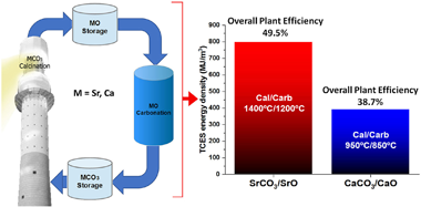
Abstract
Thermochemical energy storage (TCES) has attracted interest in the last years due to the possibility of attaining high energy densities, seasonal storage capacity and greater efficiencies than currently commercial thermal energy storage systems using molten salts. This work analyses the potential of an ultra-high temperature TCES system based on the SrCO3/SrO system. The process relies upon the reversible decomposition of SrCO3 into SrO and CO2. As proposed in previous works for the integration of the Ca-Looping process to store energy in CSP plants, both the calcination (endothermic) and carbonation (exothermic) reactions are carried out in a closed CO2 loop. At these conditions, the required temperature to attain full calcination in short residence times is around 1400 degrees C whereas carbonation takes place at about 1200 degrees C. Using this process, the energy density potentially achievable by the storage material is very high (around 2000 MJ/m(3)) while the ultra-high carbonation temperature would improve thermoelectric efficiency. The enhancement of the multicycle performance of the SrCO3/SrO system using refractory additives is also explored. Even though current commercial CSP plants with tower technology cannot yet operate at these ultra-high temperatures, recent advances in the development of high-temperature solar receivers could allow operation at 1400 degrees C in the medium term. Finally, a conceptual model of the integration of the SrCO3/SrO system in a CSP plant supports higher overall efficiency and energy density, but lower solar-to-electric efficiency due to thermal losses.
Mayo, 2022 · DOI: 10.1016/j.solmat.2022.111632
Nanotecnología en Superficies y Plasma
Influence of Femtosecond Laser Modification on Biomechanical and Biofunctional Behavior of Porous Titanium Substrates
Beltran, AM; Giner, M; Rodríguez, A; Trueba, P; Rodríguez-Albelo, LM; Vázquez-Gámez, MA; Godinho, V; Alcudia, A; Amado, JM; López-Santos, C; Yadir, TMaterials, 15 (2022) 2969 DOI: 10.3390/ma15092969
Abstract
Bone resorption and inadequate osseointegration are considered the main problems of titanium implants. In this investigation, the texture and surface roughness of porous titanium samples obtained by the space holder technique were modified with a femtosecond Yb-doped fiber laser. Different percentages of porosity (30, 40, 50, and 60 vol.%) and particle range size (100-200 and 355-500 mu m) were compared with fully-dense samples obtained by conventional powder metallurgy. After femtosecond laser treatment the formation of a rough surface with micro-columns and micro-holes occurred for all the studied substrates. The surface was covered by ripples over the micro-metric structures. This work evaluates both the influence of the macro-pores inherent to the spacer particles, as well as the micro-columns and the texture generated with the laser, on the wettability of the surface, the cell behavior (adhesion and proliferation of osteoblasts), micro-hardness (instrumented micro-indentation test, P-h curves) and scratch resistance. The titanium sample with 30 vol.% and a pore range size of 100-200 mu m was the best candidate for the replacement of small damaged cortical bone tissues, based on its better biomechanical (stiffness and yield strength) and biofunctional balance (bone in-growth and in vitro osseointegration).
Mayo, 2022 · DOI: 10.3390/ma15092969
Materiales y Procesos Catalíticos de Interés Ambiental y Energético
Characterization of Re-Mo/ZSM-5 catalysts: How Re improves the performance of Mo in the methane dehydroaromatization reaction
Lopez-Martin, A; Sini, MF; Cutrufello, MG; Caballero, A; Colon, GApplied Catalysis B-Environmental, 304 (2022) 120960 DOI: 10.1016/j.apcatb.2021.120960
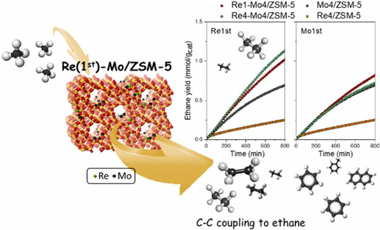
Abstract
In this study, the promoting effect of rhenium addition as a co-dopant on Mo/ZSM-5 catalysts system has been analysed. Hence, bimetallic (Re-Mo/ZSM-5) catalysts have been synthesized using a sequential impregnation methodology. The catalytic performance for direct aromatization of methane reaction has been determined and correlated with their physical and chemical state combining multiple characterization techniques. An important synergy between Mo and Re, affected by the sequential impregnation, has been observed. Thus, Re1-Mo4/ZSM-5 in which Re has been incorporated first shows notably higher aromatic yields and stability against deactivation. Characterization results suggest that catalytic enhancement is due to the important effect of Re presence in close interaction with Mo. Improved evolution of ethane through C-C coupling would be correlated to this catalytic performance. As we discuss, Mo nature and location in the bimetallic systems are strongly conditioned by Re and the impregnation sequence and favours such intermediate step.
Mayo, 2022 · DOI: 10.1016/j.apcatb.2021.120960
Materiales de Diseño para la Energía y Medioambiente
Transparent, UV-blocking, and high barrier cellulose-based bioplastics with naringin as active food packaging materials
Guzman-Puyol, S; Hierrezuelo, J; Benitez, JJ; Tedeschi, G; Porras-Vazquez, JM; Heredia, A; Athanassiou, A; Romero, D; Heredia-Guerrero, JAInternational Journal of Biological Macromolecules, 209 (2022) 1985-1994 DOI: 10.1016/j.ijbiomac.2022.04.177
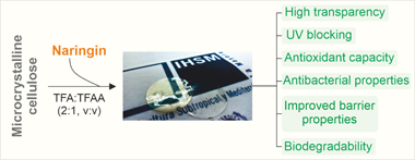
Abstract
Free-standing, robust, and transparent bioplastics were obtained by blending cellulose and naringin at different proportions. Optical, thermal, mechanical, antioxidant, and antimicrobial properties were systematically investigated. In general, the incorporation of naringin produced important UV blocking and plasticizer effects and good antioxidant and antibacterial properties. Moreover, the barrier properties were characterized by determination of their water and oxygen transmission rates, finding that both parameters decreased by increasing the naringin content and reaching values similar to other petroleum-based plastics and cellulose derivatives used for food packaging applications. Finally, the biodegradability of these films was determined by measurement of the biological oxygen demand (BOD) in seawater, demonstrating an excellent decomposition in such conditions.
Mayo, 2022 · DOI: 10.1016/j.ijbiomac.2022.04.177
Composition and technological features of ceramics manufactured by Benito de Valladares in the seventeenth century from the Alcazar Palace in Seville, Spain
Pérez-Rodríguez, J.L.; Robador, M.D.; Duran, A.European Physical Journal Plus, 137 (2022) 469 DOI: 10.1140/epjp/s13360-022-02669-9
Abstract
The walls of the Alcazar Palace in Seville have been covered with ceramic tiles of different styles that were manufactured with different techniques. Several studies have been carried out on these ceramics, but no interest has been paid to the tiles manufactured by the workshop of the Valladares family, one of the most productive ceramic workshops in Triana (Seville). In this work, tiles that were made in the Valladares workshop are studied for the first time. The tiles from the Cenador del Leon built in 1645-1646 were chosen. The experimental studies suggest that the ceramic body was manufactured with silico-calcareous clay. This raw material was heated to a temperature of ca. 900 degrees C. A nondestructive and on-site analytical procedure was applied first. Microsamples were also taken and studied through microanalytical techniques. The maiolica style was used by Benito de Valladares for tile manufacture. The glaze phases were constituted by two layers. The pigments and doping elements used to obtain different colors were characterized. Valladares' work is considered as a continuation of Augusta's work; therefore, a comparison between both ceramists has been realized to better understand the ceramics production in southern Spain during the sixteenth to seventeenth centuries.
Abril, 2022 · DOI: 10.1140/epjp/s13360-022-02669-9
Nanotecnología en Superficies y Plasma
Thin film nanostructuring at oblique angles by substrate patterning
Muñoz-Pina, S; Alcaide, AM; Limones-Ahijon, B; Oliva-Ramirez, M; Rico, V; Alcala, G; Gonzalez, MU; García-Martín, JM; Alvarez, R; Wang, D; Schaaf, P; Gonzalez-Elipe, AR; Palmero, ASurface & Coatings Technology, 436 (2022) 128293 DOI: 10.1016/j.surfcoat.2022.128293

Abstract
It is demonstrated that, besides classical nanocolumnar arrays, the oblique angle geometry induces the growth of singular structures in the nanoscale when using wisely designed patterned substrates. Well-ordered array of crosses, cylindrical nanorods or hole structures arranged in square or hexagonal regular geometries are reported as examples, among others. The fundamental framework connecting substrate topography and film growth at oblique angles is presented, allowing the use of substrate patterning as a feasible thin film nanostructuring technique. A systematic analysis of the growth of TiO2 thin films on 4 different lithographic patterned substrates in 4 different scale lengths is also presented. A first conclusion is the existence of a height-based selective growth in the initial stages of the deposition, by which the film preferentially develops on top of the tallest substrate features. This behavior is maintained until the film reaches a critical thickness, the so-called Oblivion Thickness, above which the film topography becomes gradually independent of the substrate features. A general formula relating the spatial features of the pattern, the coarsening exponent and the Oblivion Thickness has been deduced.
Abril, 2022 · DOI: 10.1016/j.surfcoat.2022.128293
Reactividad de Sólidos
Ageing-resistant zirconia/graphene-based nanostructures composites for use as biomaterials
Morales-Rodriguez, A; Gonzalez-Orellana, C; Perez-Garcia, AA; Lopez-Pernia, C; Munoz-Ferreiro, C; Poyato, R; Gallardo-Lopez, AJournal of the European Ceramic Society, 42 (2022) 1784-1795 DOI: 10.1016/j.jeurceramsoc.2021.11.060
Abstract
This work explores the incorporation of graphene-based two-dimensional nanostructures as moisture barriers to delay hydrothermal ageing of yttria-stabilized zirconia and strengthen its use in biomedical applications. Two sets of highly dense zirconia composites incorporating multilayered graphene with very different lateral dimensions, few layer graphene and exfoliated graphene nanoplatelets, were prepared. The effect of the addition of graphene nanostructures on zirconia ageing was investigated by conducting accelerated hydrothermal degradation experiments in an autoclave. An improved resistance to low-temperature degradation and a high tolerance to damage were achieved in the composites compared to those of monolithic zirconia. The incorporation of 1 vol% multilayered graphene was very effective in restricting the hydrothermal degradation. In particular, the composite incorporating exfoliated graphene nanosheets exhibited outstanding resistance to ageing because of their fine dispersion throughout the matrix, which effectively seemed to restrict grain growth and slow the propagation of the transformation front to the ceramic bulk.
Abril, 2022 · DOI: 10.1016/j.jeurceramsoc.2021.11.060
Materiales Ópticos Multifuncionales
Transparent Phosphor Thin Films Based on Rare-Earth-Doped Garnets: Building Blocks for Versatile Persistent Luminescence Materials
Castaing, V; Lozano, G; Míguez, HAdvanced Photonics Research, 3 (2022) 2100367 DOI: 10.1002/adpr.202100367
Abstract
Afterglow properties of persistent phosphors are attracting a great deal of attention in the fields of bioimaging, sensing, labeling, safety, or security. Complex garnet oxides, especially those doped with Ce3+ and Cr3+, are particularly relevant to this end since their persistent luminescence can be tuned through matrix composition and activated by visible light, in contrast to the vast majority of persistent phosphors that require UV excitation. Most extended preparation routes yield micrometer-sized phosphors that display strong light scattering, which limits their versatility and applicability. Herein, nanostructured garnet oxide-based thin films that are transparent and feature persistent luminescence properties are demonstrated. Following a sol–gel route and after high temperature annealing, few hundred nanometre-thick Y3Al2Ga3O12:Ce3+,Cr3+ transparent films showing efficient green emission and afterglow are attained. Gd3Al2Ga3O12:Ce3+,Cr3+ transparent thin films displaying yellow afterglow with distinct persistent kinetics are demonstrated, to prove the generality of the approach herein proposed. Its versatility is further demonstrated by developing layered phosphors with time-dependent chromaticity due to the unique persistent emission color – upon blue light excitation – and kinetics of each layer forming the stack. The results pave an avenue toward nanodevices and multifunctional coatings in which afterglow offers hitherto unexplored properties.
Abril, 2022 · DOI: 10.1002/adpr.202100367
Materiales y Procesos Catalíticos de Interés Ambiental y Energético
H2 Photoproduction Efficiency: Implications of the Reaction Mechanism as a Function of the Methanol/Water Mixture
Barba-Nieto, I; Colon, G; Kubacka, A; Fernandez-Garcia, MCatalysts, 12 (2022) 402 DOI: 10.3390/catal12040402
Abstract
The influence of the reaction pathway of the sacrificial molecule oxidation to generate hydrogen is here investigated for lean and rich methanol reaction mixtures. Pt-TiO2 powders promoted or not with tin sulfide were used as catalysts. With the help of in situ infrared experiments under reaction conditions, methanol evolution was shown to take place by hole-related oxidation steps, with alkoxy and carbon-centered species as key radical species. The study analyzed quantitatively the fate and chemical use of the photons absorbed by the solids with the help of the quantum efficiency and the useful fraction of photons observables. Within this framework, the role of the sulfide component to promote photoactivity is interpreted, braiding chemical and photonic information.
Abril, 2022 · DOI: 10.3390/catal12040402
Química de Superficies y Catálisis
3D-printed structured catalysts for CO2 methanation reaction: Advancing of gyroid-based geometries
Gonzalez-Castano, M; Baena-Moreno, F; De Miguel, JCN; Miah, KUM; Arroyo-Torralvo, F; Ossenbrink, R; Odriozola, JA; Benzinger, W; Hensel, A; Wenka, A; Arellano-García, HEnergy Conversion and Management, 258 (2022) 115464 DOI: 10.1016/j.enconman.2022.115464
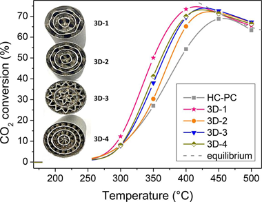
Abstract
This work investigates the CO2 methanation rate of structured catalysts by tuning the geometr y of 3D-printed metal Fluid Guiding Elements (FGEs) structures based on periodically variable pseudo-gyroid geometries. The enhanced performance showed by the structured catalytic systems is mostly associated with the capability of the FGEs substrate geometries for efficient heat usages. Thus, variations on the channels diameter resulted in ca. 25% greater CO2 conversions values at intermediate temperature ranges. The highest void fraction evidenced in the best performing catalyst (3D-1) favored the radial heat transfer and resulted in significantly enhanced catalytic activity, achieving close to equilibrium (75%) conversions at 400 ? and 120 mL/min. For the 3D-1 catalyst, a mathematical model based on an experimental design was developed thus enabling the estimation of its behavior as a function of temperature, spatial velocity, hydrogen to carbon dioxide (H-2/CO2) ratio, and inlet CO2 concentration. Its optimal operating conditions were established under 3 different scenarios: 1) no restrictions, 2) minimum H-2:CO2 ratios, and 3) minimum temperatures and H-2/CO2 ratio. For instance, for the lattest scenario, the best CO2 methanation conditions require operating at 431 ?, 200 mL/min, H-2/CO2 = 3 M ratio, and inlet CO2 concentration = 10 %.
Abril, 2022 · DOI: 10.1016/j.enconman.2022.115464
Nanotecnología en Superficies y Plasma
QUEELS: Software to calculate the energy loss processes in TEELS, REELS, XPS and AES including effects of the core hole
Tougaard, S; Pauly, N; Yubero, FSurface and Interface Analysis, 54 (2022) 820-833 DOI: 10.1002/sia.7095
Abstract
We present the user-friendly and freely available software package QUEELS (QUantitative analysis of Electron Energy Losses at Surfaces) that allows to calculate effective inelastic scattering cross sections within the dielectric response description, for swift electrons travelling nearby surfaces in several environments. We briefly describe the underlying theoretical models and illustrate its use to evaluate the distribution of energy losses taking place in electron spectroscopies like transmission electron energy loss spectroscopy (TEELS), X-ray photoelectron spectroscopy (XPS), Auger electron spectroscopy (AES) and reflection electron energy loss spectroscopy (REELS), which are widely used for material analysis. This includes the intrinsic excitations due to the core hole in XPS and AES.
Abril, 2022 · DOI: 10.1002/sia.7095
Reactividad de Sólidos
Highly uniform Y3Al2Ga3O12-based nanophosphors for persistent luminescence bioimaging in the visible and NIR regions
Arroyo, E; Herrero, BT; De la Fuente, JM; Ocaña, M; Becerro, AIInorganic Chemistry Frontiers, 9 (2022) 2454-2461 DOI: 10.1039/d2qi00480a
Abstract
In the last few years, persistent phosphors with a garnet crystal structure have attracted a great deal of interest for a plethora of applications ranging from bioimaging to anti-counterfeiting technologies. However, the development of synthesis methods to fabricate uniform garnet-based micro and nanoparticles, that are needed for such applications, is not mature at all. This study reports the synthesis of highly uniform yttrium aluminum gallium garnet nanospheres. The method is based on homogeneous precipitation in a polyol medium followed by silica coating and calcination. The nanoparticles resulting after silica removal were also uniform and were easily functionalized with polyacrylic acid. The colloidal stability of the latter in physiological media and their biocompatibility were analyzed. The luminescence of the particles, doped with Ce3+, Cr3+, and Nd3+, was studied by recording emission and excitation spectra and persistent luminescence decay curves. Due to their uniform morphology, high colloidal stability, absence of toxicity, and persistent emission in the visible and near-infrared regions, the reported nanospheres show great potential as persistent luminescent bioimaging probes. In addition, the synthesis method paves the way for future use of this persistent material in other applications that require the phosphor to be in the form of highly uniform nanoparticles.
Abril, 2022 · DOI: 10.1039/d2qi00480a
Fotocatálisis Heterogénea: Aplicaciones
Fast photodegradation of rhodamine B and caffeine using ZnO-hydroxyapatite composites under UV-light illumination
KarimTanji, J.A.Navio, Abdellah Chaqroune, Jamal Naja, F.Puga, M.C.Hidalgo, AbdelhakKherbecheCatalysis Today, 388 (2022) 176-186 DOI: 10.1016/j.cattod.2020.07.044
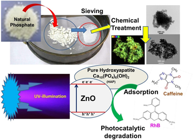
Abstract
Zinc oxide-hydroxyapatite composites were prepared using wet impregnation method. Firstly, a natural phosphate ore rich in silica and calcium phosphate was sieved to separate silica phase from phosphate phase. Then, through a chemical precipitation method, a pure hydroxyapatite (HAP) was obtained, which was used as a support for ZnO immobilization and applied for the photodegradation of two toxic contaminants: a transparent molecule (caffeine) and dye molecule (rhodamine B). During the present work two weight ratio percentages of zinc oxide were used: 25 wt.% and 50 wt.% of ZnO relative to HAP. The samples were characterized by X-ray diffraction (XRD), Fourier Transform Infrared (FTIR), X-ray Fluorescence (XRF), BET surface area (SBET), Scanning Electron Microscopy (SEM-EDS) and by Transmission Electron Microscopy (TEM-STEM). The immobilization of ZnO on HAP surface followed by thermal treatment at 400 °C for 2 h to get a homogenous dispersion of ZnO on the hydroxyapatite support. At high ZnO impregnation percentage, photodegradation performances of ZnO-HAP under UV illumination were fast and superior than the ZnO photocatalyst alone. The results showed that due to the presence of HAP, the conversion of both molecules became faster and greater, since it promotes the synergic phenomena of adsorption and photocatalysis. The toxicity of the treated substrate solutions obtained in the corn kernels germination test indicated a low toxicity after the photodegradation processes, probably due to a high mineralization degree.
Abril, 2022 · DOI: 10.1016/j.cattod.2020.07.044
Fotocatálisis Heterogénea: Aplicaciones
Z-scheme WO3/PANI heterojunctions with enhanced photocatalytic activity under visible light: A depth experimental and DFT studies
Y. Naciri; A.Hsini; A.Bouziani; K.Tanji; B.El Ibrahimi; M.N.Ghazza; B. Bakiz; A.Albourine; A.Benlhachemi; J.A. NavíoChemosphere, 292 (2022) 133468 DOI: 10.1016/j.chemosphere.2021.133468
Abstract
A WO3@PANI heterojunction photocatalyst with a various mass ratio of polyaniline to WO3 was obtained via the in situ oxidative deposition polymerization of aniline monomer in the presence of WO3 powder. The characterization of WO3@PANI composites was carried via X-ray diffraction (XRD), scanning electron microscopy (SEM-EDS), transmission electron microscopy (TEM), Fourier transform infrared spectroscopy (FT-IR), ultraviolet–visible diffuse reflection spectroscopy (DRS), X-ray photoelectron spectroscopy (XPS) and photoluminescence spectroscopy (PL). The photocatalytic efficiency of WO3@PANI photocatalysts was assessed by following the decomposition of the Rhodamine B (RhB) dye under visible light irradiation (λ >420 nm). The results evidenced the high efficiency of the WO3@PANI (0.5 wt %) nanocomposite in the photocatalytic degradation of RhB (90% within 120 min) under visible light irradiation 3.6 times compared to pure WO3. The synergistic effect between PANI and WO3 is the reason for the increased photogenerated carrier separation. The superior photocatalytic performance of the WO3@PANI catalyst was ascribed to the increased visible light in the visible range and the efficient charge carrier separation. Furthermore, the Density Functional Theory study (DFT) of WO3@PANI was performed at the molecular level, to find its internal nature for the tuning of photocatalytic efficiency. The DFT results indicated that the chemical bonds connected the solid-solid contact interfaces between WO3 and PANI. Finally, a plausible photocatalytic mechanism of WO3@PANI (0.5 wt %) performance under visible light illumination is suggested to guide additional photocatalytic activity development.
Abril, 2022 · DOI: 10.1016/j.chemosphere.2021.133468
Nanotecnología en Superficies y Plasma
Ionomer-Free Nickel-Iron bimetallic electrodes for efficient anion exchange membrane water electrolysis
Lopez-Fernandez, E; Gomez-Sacedon, C; Gil-Rostra, J; Espinos, JP; Gonzalez-Elipe, AR; Yubero, F; De Lucas-Consuegra, AChemical Engineering Journal, 433 (2022) 133774 DOI: 10.1016/j.cej.2021.133774
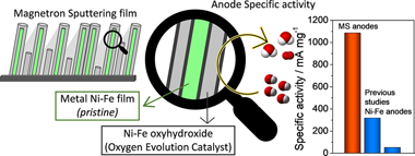
Abstract
A bottleneck for the deployment of the Anion Exchange Membrane Water Electrolysis (AEMWE) is the manufacturing of efficient and long lasting anodes and cathodes for the cells. Highly performant bimetallic Ni/Fe catalyst films with various atomic ratios have been prepared by magnetron sputtering in an oblique angle configuration (MS-OAD) and used as anodes for AEMWE. Electrocatalytic experiments in a small three-electrode cell and a thorough analysis of the electrode properties with various physico-chemical characterization tech-niques have been used to select the nanostructured anode catalyst which, depicting an optimized Ni/Fe ratio, presents the maximum activity for the oxygen evolution reaction. These anode layers are then scale-up for their integration in an AEMWE cell where the influence of assembly conditions and the effect of adding an ionomer to the anodes have been studied. The obtained results have demonstrated the outstanding properties of the fabri-cated bimetallic films in terms of activity, stability, and operation under ionomer-free conditions. Current density values around 400 and 600 mA cm(-2) at 40??& nbsp;and 60 C (2.0 V), respectively, much higher than those obtained with pure Ni, were obtained with an optimized membrane electrode assembly. The high yield obtained with these electrodes gains further relevance when considering that the current yield per unit mass of the anodic active phase catalyst (i.e., 1086 mA mg(-1) at 2.0 V and 40??) is the highest among equivalent values reported in literature. The possibilities and prospects of the use of bimetallic catalyst films prepared by MS-OAD for AEMWE are discussed.
Abril, 2022 · DOI: 10.1016/j.cej.2021.133774
Fotocatálisis Heterogénea: Aplicaciones
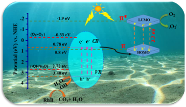
Insights into the structural and physicochemical properties of Zn-Bi-O composites for efficient photodegradation of caffeic acid, rhodamine B and methyl orange
F.Puga; J.A.Navío; J.M.Córdoba; F.Romero-Sarria; M.C.HidalgoApplied Surface Science, 581 (2022) 152351 DOI: 10.1016/j.apsusc.2021.152351
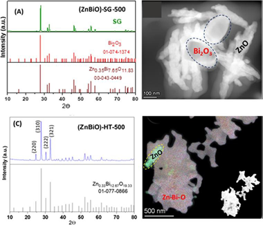
Abstract
Different Zn-Bi-O composites were synthesized following the starting chemical molar composition of ZnBi2O4 spinels by a sol–gel method, (ZnBiO)-SG, and its subsequent hydrothermal treatment, (ZnBiO)-HT. The acquired X-ray diffractograms after sequential thermal treatments at a programmed rate indicate that both precursors evolved, after calcination at 500 °C, to materials (ZnBiO) with different stoichiometry. The use of different characterization techniques (both FT-IR and TEM), allowed us to establish that, with the sol–gel process a mixed ZnO/Bi2O3 oxide is generated, while after hydrothermal process a ternary Zn-Bi-O oxide is formed, with small amounts of residual ZnO. The photocatalytic properties of the synthesized samples were evaluated using Caffeic acid, Rhodamine B and Methyl Orange as model substrates. It can be concluded that both catalysts showed excellent photocatalytic activity for the degradation of trans-caffeic acid under both UV and visible illumination. The leaching process (in particular of zinc), which is produced with the illumination time (in particular under UV illumination) in the presence of oxygen, raises the hypothesis of a foreseeable formation of complexes (photochemically stable or unstable) of caffeic acid with Zn2+ and Bi3+ ions. The plausible donor/acceptor interactions between the toxic molecules studied and the Zn2+ and Bi3+ ions, could condition the degradation processes, by means of a photoassisted process that would take place both, in the heterogeneous (photocatalytic) and homogeneous (photoassisted) phases. For the degradation processes of Rhodamine B and Methyl Orange, additional experimental conditions are studied that significantly improved their photocatalytic degradation.
Abril, 2022 · DOI: 10.1016/j.apsusc.2021.152351
Materiales Ópticos Multifuncionales
Enhanced up-conversion photoluminescence in fluoride-oxyfluoride nanophosphor films by embedding gold nanoparticles
Ngo, TT; Lozano, G; Miguez, HMaterials Advances 3 (2022) 4235-4242 DOI: 10.1039/D2MA00068G
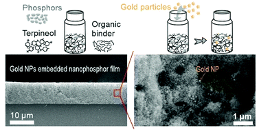
Abstract
Owing to their unique non-linear optical character, lanthanide-based up-converting materials are potentially interesting for a wide variety of fields ranging from biomedicine to light harvesting. However, their poor luminescent efficiency challenges the development of technological applications. In this context, localized surface plasmon resonances (LSPRs) have been demonstrated as a valuable strategy to improve light conversion. Herein, we utilize LSPR induced by gold nanoparticles (NPs) to enhance up-conversion photoluminescence (UCPL) in transparent, i.e. scattering-free, films made of nanophosphors formed by fluoride–oxyfluoride host matrix that feature high thermal stability. Transparency allows excitation by an external source without extinction losses caused by unwanted diffuse reflection. We provide a simple method to embed gold NPs in films made of YF/YOF:Yb3+,Er3+ UC nanophosphors, via preparation of a viscous paste composed of both UC nanophosphors and colloidal gold NPs, reducing complexity in sample fabrication. The dimensions of gold NPs are such that their associated LSPR matches spectrally with the green emission band of the Er3+ doped nanophosphors. In order to demonstrate the benefits of plasmonic nanoparticles for UCPL in nanophosphor films, we provide a careful analysis of the structural properties of the composite thin films along with precise characterization of the impact of the gold NPs on the photophysical properties of UC nanophosphors.
Abril, 2022 · DOI: 10.1039/D2MA00068G
Materiales de Diseño para la Energía y Medioambiente
Structural analysis of mixed alpha- and beta-amyrin samples
Gomez-Pulido, LDM; Gonzalez-Cano, RC; Benitez, JJ; Dominguez, E; Heredia, ARoyal Society Open Science, 9 (2022) 211787 DOI: 10.1098/rsos.211787
Abstract
Little is known about the structure and molecular arrangement of alpha- and beta-amyrin, a class of triterpenoids found within the cuticle of higher plants. Blends of both amyrin isomers with different ratios have been studied taking into consideration a combined methodology of density functional theory (DFT) calculations with experimental data from scanning electron microscopy, differential scanning calorimetry and Raman vibrational spectroscopy. Results indicate that trigonal trimeric aggregations of isomer mixtures are more stable, especially in the 1 : 2 (alpha : beta) ratio. A combination of Raman spectroscopy and DFT calculations has allowed to develop an equation to determine the amount of beta-amyrin in a mixed sample.
Abril, 2022 · DOI: 10.1098/rsos.211787
Materiales de Diseño para la Energía y Medioambiente
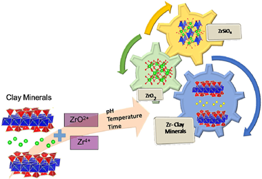
Insight into the role of temperature, time and pH in the effective zirconium retention using clay minerals
Pavon, E; Alba, MDJournal of Environmental Chemical Engineering, 308 (2022) 114635 DOI: 10.1016/j.jenvman.2022.114635
Abstract
The use of zirconium in chemical industries generates a potential risk of Zr contamination in the environment, with particular concern for the decommissioning of uranium-graphite reactors. Among the natural adsorbents employed for the treatment of nuclear waste, clay minerals showed a very high affinity adsorption for radionuclides, but the influence of the chemical composition, pressure, temperature and time reaction have not yet been analysed on deep. Thus, the objective of this research is to explore several experimental conditions for an actual prediction of the behaviour of zirconium immobilization by clay minerals. The results have shown that factors such as zirconium cation nature (Zr4+ or ZrO2+), temperature, time and pH influence the extent of zirconium immobilization by clay minerals and the zirconium phases generated. At moderate conditions, zirconium tectosilicates are formed and evolve to zircon at high temperature and a longer time reaction.
Abril, 2022 · DOI: 10.1016/j.jenvman.2022.114635
Materiales para Bioingeniería y Regeneración Tisular
Mesoporous Silica-Based Nanoparticles as Non-Viral Gene Delivery Platform for Treating Retinitis Pigmentosa
Valdes-Sanchez, L; Borrego-González, S; Montero-Sanchez, A; Massalini, S; De la Cerda, B; Díaz-Cuenca, A; Díaz-Corrales, FJJournal of Clinical Medicine, 11 (2022) 2170 DOI: 10.3390/jcm11082170
Abstract
Background: Gene therapy is a therapeutic possibility for retinitis pigmentosa (RP), in which therapeutic transgenes are currently delivered to the retina by adeno-associated viral vectors (AAVs). Although their safety and efficacy have been demonstrated in both clinical and preclinical settings, AAVs present some technical handicaps, such as limited cargo capacity and possible immunogenicity in repetitive doses. The development of alternative, non-viral delivery platforms like nanoparticles is of great interest to extend the application of gene therapy for RP. Methods: Amino-functionalized mesoporous silica-based nanoparticles (N-MSiNPs) were synthesized, physico-chemically characterized, and evaluated as gene delivery systems for human cells in vitro and for retinal cells in vivo. Transgene expression was evaluated by WB and immunofluorescence. The safety evaluation of mice subjected to subretinal injection was assessed by ophthalmological tests (electroretinogram, funduscopy, tomography, and optokinetic test). Results: N-MSiNPs delivered transgenes to human cells in vitro and to retinal cells in vivo. No adverse effects were detected for the integrity of the retinal tissue or the visual function of treated eyes. N-MSiNPs were able to deliver a therapeutic transgene candidate for RP, PRPF31, both in vitro and in vivo. Conclusions: N-MSiNPs are safe for retinal delivery and thus a potential alternative to viral vectors.
Abril, 2022 · DOI: 10.3390/jcm11082170
Materiales de Diseño para la Energía y Medioambiente
Strength and thermal shock resistance of fiber-bonded Si-Al-C-O and Si-Ti-C-O ceramics
Vera, MC; Martinez-Fernandez, J; Singh, M; Ramirez-Rico, JInternational Journal of Applied Ceramic Technology, 19 (2022) 1126-1135 DOI: 10.1111/ijac.13928
Abstract
Silicon carbide-based fiber-bonded ceramics, obtained from hot pressing of woven silicon carbide fibers, are a cost-effective alternative to ceramic-matrix composites due to their ease of fabrication, involving few processing steps, and competitive thermomechanical properties. In this work, we studied the high-temperature strength and thermal shock resistance of Si-Al-C-O and Si-Ti-C-O fiber-bonded SiC ceramics obtained from hot pressing of two types of ceramic fibers, by mechanical testing in four-point bending. The bending strength of Si-Al-C-O-based fiber-bonded ceramics at room temperature is similar to 250-260 MPa and remains constant with temperature, while the bending strength of Si-Ti-C-O increases slightly from the initial 220 to similar to 250 MPa for the highest temperature. Both materials retain up to 90% of their room temperature strength after thermal shocks of 1400 degrees C and show no reduction in elastic moduli. After thermal shock, failure mode is the same as in the case of as-received materials.
Marzo, 2022 · DOI: 10.1111/ijac.13928
Reactividad de Sólidos
A novel Multi-Phase Flash Sintering (MPFS) technique for 3D complex-shaped ceramics
Molina-Molina, S; Gil-Gonzalez, E; Duran-Olivencia, FJ; Valverde, JM; Perejon, A; Sanchez-Jimenez, PE; Pérez-Maqueda, LAApplied Materials Today, 26 (2022) 101274 DOI: 10.1016/j.apmt.2021.101274
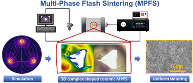
Abstract
This work demonstrates the first proof-of-concept of Multi-Phase Flash Sintering (MPFS). This novel technique essentially consists of applying a rotating electric field to the sample by means of a multi-phase voltage source as furnace temperature increases. Several ceramic materials with different types of electrical conductivities are sintered within seconds at furnace temperatures much lower than those used for traditional DC flash sintering due to the higher power densities administered by a multi-phase power supply. Thus, ceramic materials are flashed at relatively lower applied voltages which minimizes undesired phenomena such as localization and preferential current pathways. Furthermore, MPFS allows diverse electrode configurations to promote a more uniform electric field distribution, enhancing the sintering of 3D complex-shaped specimens. MPFS could be a true breakthrough in materials processing, as 3D complex-shaped specimens are homogeneously sintered at reduced temperatures, while keeping all the advantages of conventional flash sintering.
Marzo, 2022 · DOI: 10.1016/j.apmt.2021.101274
Nanotecnología en Superficies y Plasma
Multiscale ultrafast laser texturing of marble for reduced surface wetting
Ariza, R; Alvarez-Alegria, M; Costas, G; Tribaldo, L; Gonzalez-Elipe, AR; Siegel, J; Solis, JApplied Surface Science, 577 (2022) 152850 DOI: 10.1016/j.apsusc.2021.151850
Abstract
The modification of the wetting properties of marble surfaces upon multi-scale texturing induced by ultrafast laser processing (340 fs pulse duration, 1030 nm wavelength) has been investigated with the aim of evaluating its potential for surface protection. The contact angle (CA) of a water drop placed on the surface was used to assess the wettability of the processed areas. Although the surfaces are initially hydrophilic upon laser treatment, after a few days they develop a strong hydrophobic behavior. Marble surfaces have been irradiated with different scan line separations to elucidate the relative roles of multi-scale roughness (nano-and micro-texture) and chemical changes at the surface. The time evolution of the contact angle has been then monitored up to 11 months after treatment. A short and a long-term evolution, associated to the combined effect of multi-scale roughness and the attachment of chemical species at the surface over the time, have been observed. XPS and ATR measurements are consistent with the progressive hydroxylation of the laser treated surfaces although the additional contribution of hydrocarbon adsorbates to the wettability evolution cannot be ruled-out. The robustness of the results has been tested by CA measurements after cleaning in different conditions with very positive results.
Marzo, 2022 · DOI: 10.1016/j.apsusc.2021.151850
Nanotecnología en Superficies y Plasma
Rhodamine 6G and 800 intermolecular heteroaggregates embedded in PMMA for near-infrared wavelength shifting
Castillo-Seoane, J; Gonzalez-García, L; Obrero-Pérez, JM; Aparicio, FJ; Borras, A; Gonzalez-Elipe, AR; Barranco, A; Sanchez-Valencia, JRJournal of Materials Chemistry C, 10 (2022) 7119-7131 DOI: 10.1039/d1tc06167d
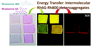
Abstract
The opto-electronic properties of small-molecules and functional dyes usually differ when incorporated into solid matrices with respect to their isolated form due to an aggregation phenomenon that alters their optical and fluorescent properties. These spectroscopic modifications are studied in the framework of the exciton theory of aggregates, which has been extensively applied in the literature for the study of molecular aggregates of the same type of molecules (homoaggregation). Despite the demonstrated potential of the control of the heteroaggregation process (aggregation of different types of molecules), most of the reported works are devoted to intramolecular aggregates, complex molecules formed by several chromophores attached by organic linkers. The intramolecular aggregates are specifically designed to hold a certain molecular structure that, on the basis of the exciton theory, modifies their optical and fluorescent properties with respect to the isolated chromophores that form the molecule. The present article describes in detail the incorporation of Rhodamine 6G (Rh6G) and 800 (Rh800) into polymeric matrices of poly-(methyl methacrylate), PMMA. The simultaneous incorporation of both dyes results in an enhanced fluorescent emission in the near-infrared (NIR), originating from the formation of ground-state Rh6G-Rh800 intermolecular heteroaggregates. The systematic control of the concentration of both rhodamines provides a model system for the elucidation of the heteroaggregate formation. The efficient energy transfer between Rh6G and Rh800 molecules can be used as wavelength shifters to convert effectively the light from visible to NIR, a very convenient wavelength range for many practical applications which make use of inexpensive commercial detectors and systems.
Marzo, 2022 · DOI: 10.1039/d1tc06167d
Química de Superficies y Catálisis
Analysis of Dry Reforming as direct route for gas phase CO2 conversion. The past, the present and future of catalytic DRM technologies
le Sache, E; Reina, TRProgress in Energy and Combustion Science, 89 (2022) 100970 DOI: 10.1016/j.pecs.2021.100970
Abstract
Transition to low carbon societies requires advanced catalysis and reaction engineering to pursue green routes for fuels and chemicals production as well as CO2 conversion. This comprehensive review provides a fresh perspective on the dry reforming of methane reaction (DRM) which constitutes a straightforward approach for effective CO2 conversion to added value syngas. The bottleneck for the implementation of this process at industrial scale is the development of highly active and robust heterogeneous catalysts able to overcome the CO2 activation barrier and deliver sufficient amount of the upgrading products at the desired operation conditions. Also, its high energy demand due to the endothermic nature of the reaction imposes extra difficulties. This review critically discusses the recent progresses on catalysts design ranging from traditional metal-supported catalysts to advanced structured and nanostructured systems with promising performance. The main advantages and culprits of the different catalytic systems are introduced aiming to inspire the catalysis community to further refine these formulations towards the development of "supercatalysts" for DRM. Besides the design of increasingly complex catalyst morphologies as well as other promising alternatives aiming at reducing the energy consumption of the process or tackle deactivation through reactor design are introduced.
Marzo, 2022 · DOI: 10.1016/j.pecs.2021.100970
Materiales y Procesos Catalíticos de Interés Ambiental y Energético
Research on properties and catalytic behaviour in CO hydrogenation at atmospheric and high pressure of bimetallic systems (10%Co+0.5%Pd)/TiO2 (Al2O3)
Shopska, M; Caballero, A; Platero, F; Todorova, S; Tenchev, K; Fabian, M; Aleksieva, K;Kolev, H; Kadinov, GReaction Kinetics Mechanisms and Catalysis, 135 (2022) 589-618 DOI: 10.1007/s11144-022-02194-x
Abstract
The properties of prereduced (10%Co + 0.5%Pd)/Al2O3 (TiO2) systems in the CO hydrogenation reaction at atmospheric and high pressure were studied. At atmospheric pressure, alumina-supported catalysts were more selective toward methane but those using titania were more active. Alumina containing samples demonstrated high temperature H-2 desorption, firmly held surface carbonate species, high tendency to agglomeration. During the reaction metal surface reconstruction and increased formation of CH2 groups occurred being more pronounced with titania-supported catalysts. Stability tests at 250 degrees C showed opposite behaviour of both systems. Monodentate carbonate intermediates adsorbed on sites of moderate strength prevailed on titania samples, while formate species predominated on high strength sites of alumina-supported catalysts. High pressure catalytic tests revealed dependence of activity on T-red, synthesis of C2+ hydrocarbons, decreased CO2 production, a higher CH4/CO2 ratio for alumina containing system. Due to SMSI, increased CO2 production on titania samples was preserved. Titania-supported catalysts revealed a stronger decrease of CO conversion rising T-red while alumina catalysts had almost unchanged activity. CO conversion decreased with time due to difficulties in surface diffusion of reagents/intermediates/products and metal particle agglomeration. Concerning T-red comparison of product distribution showed a steady trend. Because of stable CO and CHx surface species, titania containing catalysts produced lower content of C5+ compounds. Alumina-supported samples showed a higher selectivity to C5+ compounds at the expense of methane. A higher selectivity ratio for CH4 and CO2 determined in catalytic CO hydrogenation over a certain catalyst at atmospheric pressure could indicate that a given sample is predisposed to form C2+ hydrocarbons at a higher pressure.
Marzo, 2022 · DOI: 10.1007/s11144-022-02194-x
Nanotecnología en Superficies y Plasma - Materiales Nanoestructurados y Microestructura
Highly Anisotropic Organometal Halide Perovskite Nanowalls Grown by Glancing-Angle Deposition
Castillo-Seoane, J; Contreras-Bernal, L; Obrero-Perez, JM; Garcia-Casas, X; Lorenzo-Lazaro, F; Aparicio, FJ; Lopez-Santos, C; Rojas, TC; Anta, JA; Borras, A; Barranco, A; Sanchez-Valencia, JRAdvanced Materials (2022) 2107739 DOI: 10.1002/adma.202107739
Abstract
Polarizers are ubiquitous components in current optoelectronic devices as displays or photographic cameras. Yet, control over light polarization is an unsolved challenge, since the main drawback of the existing display technologies is the significant optical losses. In such a context, organometal halide perovskites (OMHP) can play a decisive role given their flexible synthesis with tunable optical properties such as bandgap and photoluminescence, and excellent light emission with a low non-radiative recombination rate. Therefore, along with their outstanding electrical properties have elevated hybrid perovskites as the material of choice in photovoltaics and optoelectronics. Among the different OMHP nanostructures, nanowires and nanorods have lately arisen as key players in the control of light polarization for lighting or detector applications. Herein, the fabrication of highly aligned and anisotropic methylammonium lead iodide perovskite nanowalls by glancing-angle deposition, which is compatible with most substrates, is presented. Their high alignment degree provides the samples with anisotropic optical properties such as light absorption and photoluminescence. Furthermore, their implementation in photovoltaic devices provides them with a polarization-sensitive response. This facile vacuum-based approach embodies a milestone in the development of last-generation polarization-sensitive perovskite-based optoelectronic devices such as lighting appliances or self-powered photodetectors.
Marzo, 2022 · DOI: 10.1002/adma.202107739
Química de Superficies y Catálisis
Understanding the promotional effect of Pt/CeO2 in cobalt-catalyzed Fischer-Tropsch synthesis using operando infrared spectroscopy at moderated pressures
Bobadilla, LF; Egana, A; Castillo, R.; Romero-Sarria, F.; Centeno, M.A.; Sanz, O.; Montes, M.; Odriozola, J.A.FUEL, 312 (2022) 122964 DOI: 10.1016/j.fuel.2021.122964
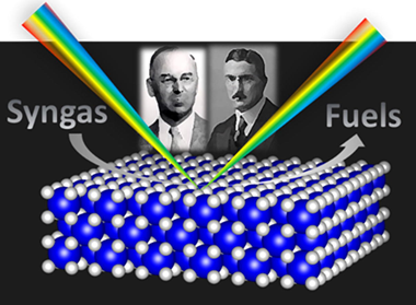
Abstract
Fischer-Tropsch (FTS) reaction is a well-known catalytic process for the conversion of synthesis gas into liquid fuels. The addition of a water gas shift (WGS) catalyst to the FTS one has been postulate to notably increase the efficiency of the process. In order to investigate this issue, we conducted the FTS reaction over a Co-Re/Al2O3 catalyst combined with an optimal WGS Pt/CeO2 catalyst. We observed a notable increase of CO conversion in presence of the Pt/CeO2 catalyst that a priori could be attributed to the WGS reaction. However, the WGS reaction is unfavourable at pressures higher than 1 bar and CO/CO2 hydrogenation over Pt/CeO2 could be more favoured under FTS reaction conditions. In order to gain insights on this fact and elucidate the role of Pt/CeO2 in the FTS reaction we have performed an operando DRIFTS-MS study under close FTS reaction conditions at 4 bar over the Pt/CeO2 catalyst.
Marzo, 2022 · DOI: 10.1016/j.fuel.2021.122964
Materiales y Procesos Catalíticos de Interés Ambiental y Energético
Preferential CO oxidation in hydrogen-rich gases over Ag catalysts supported on different supports
Todorova, S; Kolev, H; Karakirova, Y; Filkova, D; Grahovski, B; Aleksieva, K; Holgado, JP; Kadinov, G; Caballero, AReaction Kinetics Mechanisms and Catalysis, 135 (2022) 1405-1422 DOI: 10.1007/s11144-022-02158-1
Abstract
The monometallic silver supported on SiO2, Al2O3, ZSM-5 (Si:Al = 100) and bi-metallic AgCe/SiO2 samples were studied in the reaction of the preferential CO oxidation. It was established that the supported silver catalysts are promising systems for selective oxidation of CO at low temperatures and the addition of cerium oxide increases the catalytic activity and selectivity most probably because of the increase in the silver dispersion; the homogeneous distribution of Ag and ceria on the silica support; formation of Ag-n(delta+) clusters; increase in bulk and subsurface oxygen.
Marzo, 2022 · DOI: 10.1007/s11144-022-02158-1
Reactividad de Sólidos
Predictions of polymer thermal degradation: relevance of selecting the proper kinetic model
Sanchez-Jimenez, PE; Perejon, A; Arcenegui-Troya, J; Perez-Maqueda, LAJournal of Thermal Analysis and Calorimetry, 147 (2022) 2335-2341 DOI: 10.1007/s10973-021-10649-x
Abstract
Making predictions, such as lifetime estimations, is one of the main objectives of kinetic studies. Thus, from conventional thermal analysis experiments, the behavior of polymeric materials under processing or application conditions, usually far away from those used in the laboratory experiments, could be estimated. Conventional prediction procedures usually make use of oversimplified equations based on simple approaches. One of the most common approaches is the assumption of a first, or n-order, kinetic model for the process. However, recent studies have shown, for a number of polymers, that random scission kinetic models are not only physically sound, but more reliable in terms of describing the degradation kinetics. In this paper, the consequences of selecting an erroneous kinetic model on lifetime predictions is discussed. It is demonstrated, using both simulated and experimental data, that any kinetic analysis of a chain scission driven reaction performed assuming a first-order model entails enormous deviations in predictions. This occurs despite the fact that the first-order kinetic model can fit experimental data from chain scission driven reactions with significant correlation coefficients, and even lead to a reasonably good reconstruction of the original experimental curves.
Febrero, 2022 · DOI: 10.1007/s10973-021-10649-x
Materiales de Diseño para la Energía y Medioambiente
Iron-catalyzed graphitization for the synthesis of nanostructured graphitic carbons
Hunter, RD; Ramirez-Rico, J; Schnepp, ZJournal of Materials Chemistry A, 10 (2022) 4489-4516 DOI: 10.1039/d1ta09654k
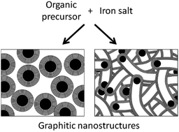
Abstract
Carbons are versatile and diverse materials that have numerous applications across energy and environmental sciences. Carbons with a graphitic structure are particularly appealing due to their high chemical stability, large surface areas and high thermal and electronic conductivity. Numerous methods exist to produce nanostructured graphitic carbons but some of these can be energy-intensive and/or have problems with scalability. One option that is being increasingly explored is the process of iron-catalyzed graphitization. This simply involves the pyrolysis of carbon-rich precursors in the presence of an iron catalyst and has been used to produce carbons with a wide range of structures and properties. This review will examine the current field of iron-catalyzed graphitization, with a focus on molecular organic or biomass precursors. Bio-derived precursors are particularly attractive as a potential option for sustainable production of graphitic carbons. We start with a brief introduction to some key carbon structures, the current applications in which they are employed and some of the key methods that have been developed to produce nanostructured graphitic carbons. We will then review the history of catalytic graphitization before evaluating the wide range of conditions and precursors that have been employed in catalytic graphitization. Finally, this review will investigate the current challenges facing iron-catalyzed graphitization, looking particularly at the limitations of the current understanding of the mechanistic aspects of graphitization, with a view to outlining where research in this field might progress.
Febrero, 2022 · DOI: 10.1039/d1ta09654k
Nanotecnología en Superficies y Plasma
Plasma assisted CO2 dissociation in pure and gas mixture streams with a ferroelectric packed-bed reactor in ambient conditions
Navascues, P; Cotrino, J; Gonzalez-Elipe, AR; Gomez-Ramirez, AChemical Engineering Journal, 430 (2022) 133066 DOI: 10.1016/j.cej.2021.133066
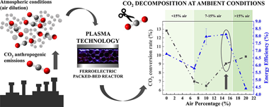
Abstract
Carbon dioxide decomposition is a challenging target to combat climate change. Nonthermal plasmas are advantageous for this purpose because they operate at ambient conditions and can be easily scaled-up. In this study, we attempt the CO2 splitting into CO and O-2 in a parallel plate packed-bed plasma reactor moderated with Lead Zirconate Titanate (PZT) as fermelectric component, achieving conversion rates and energy efficiencies higher than those obtained with BaTiO3 in our experimental device. The analysis of the reaction mechanisms with optical emission spectroscopy under various operating conditions has shown a direct correlation between energy efficiency and intensity of CO* emission bands. These results and those obtained with a LiNbO3 plate placed onto the active electrode suggest that high temperature electrons contribute to the splitting of CO2 through an enhancement in the formation of CO2+ intermediate species. Results obtained for CO2 + O-2 mixtures confirm this view and suggest that back recombination processes involving CO and O-2 may reduce the overall splitting efficiency. The study of mixtures of CO2 and dry air has proved the capacity of fermelectric packed-bed reactors to efficiently decompose CO2 with no formation of harmful NxOy subproducts in conditions close to those in real facilities. The found enhancement in energy efficiency with respect to that found for the pure gas decomposition supports that new reaction pathways involving nitrogen molecules are contributing to the dissociation reaction. We conclude that PZT moderated packed-bed plasma reactors is an optimum alternative for the decompositon of CO2 in real gas flows and ambient conditions.
Febrero, 2022 · DOI: 10.1016/j.cej.2021.133066
- ‹ anterior
- 7 of 37
- siguiente ›


![]()
icms